-
- Week4 Overview
- My Personal assignment
- Summarize the core knowledge points of PCB learning.
- Tools,Software &Machine Introduction
- Learn the Schematic of Quentorres
- Learn the PCB files of Quentorres
- From Gerber to G-Code
- Machining the PCB
- Make the BOM for QT PCB
- Solder components onto the PCB
- Test the PCB
- Write and test the program
- Team assignment
- Assignment files
week04-Electronics Production
Week 4 - Overview
In the fourth week of my study, I learned about the following aspects of PCBs:
1.The development of PCB manufacturing technology.
2.How to machine a prototype PCB (QT) using CNC.
3.The schematics, engineering drawings, and various component diagrams of PCBs.
4.Knowledge about PCB thickness,grid,layers,width,pads,nets,etc.
5.Hands-on experience with machining a PCB using a small CNC.
6.Soldering various components onto the PCB board.
Starting this week, we need to complete two projects: a team assignment and an individual assignment.
characterize the design rules for your in-house PCB production process
Link to our group page: Week4 Group Assignment
1.make and test a microcontroller development board
2.extra credit: personalize the board
3.extra credit: make it with another process
Reference Links
Week4 Electronics Production Guide for my Fab Academy Journey.My personal assignment
1.Summarize the core knowledge points of PCB learning.
1.PCB Manufacturing Technology Development:
Innovations include advancements in materials used (like high-frequency laminates for better performance), improvements in layer count and board thickness for miniaturization, and enhanced precision in trace width for high-density interconnect (HDI) boards.
Additionally, methods like Surface Mount Technology (SMT) have revolutionized how components are mounted on the boards.
This process is suitable for rapid prototyping because it allows designers to test and modify their designs quickly.
This schematic is then translated into a physical board layout, specifying the placement of components and the routing of electrical traces.
Engineering drawings may also include dimensions, specifications for drilling, and notes on tolerances and materials.
The number of layers can range from a single layer to more than a dozen in complex electronic products.
Trace width is critical for determining the current-carrying capacity of the traces and avoiding heat buildup.
Pads and Nets are the small areas of copper where components are soldered to the board, and nets are the electrical connections between them.
The CNC then mills the board based on these paths.
It's a precise process that requires careful setup and calibration.
Techniques vary from manual soldering for prototypes and small batches to automated processes like reflow soldering for production.
Proper soldering is crucial for reliable electrical connections.
2.Tools、Software &Machine Introduction
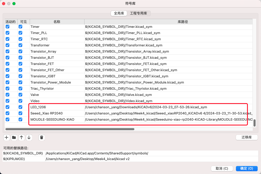
Software:Kicad
KiCad is a free and open-source electronics design automation (EDA) suite.
It features schematic capture, integrated circuit simulation, printed circuit board (PCB) layout, 3D rendering, and plotting/data export to numerous formats.
KiCad also includes a high-quality component library featuring thousands of symbols, footprints, and 3D models.
KiCad has minimal system requirements and runs on Linux, Windows, and macOS.
Learn the various functions of KiCad.

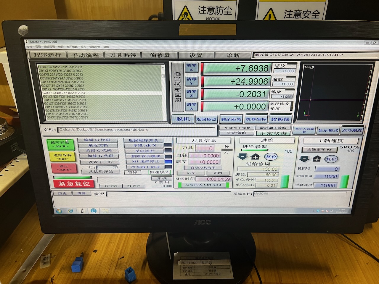
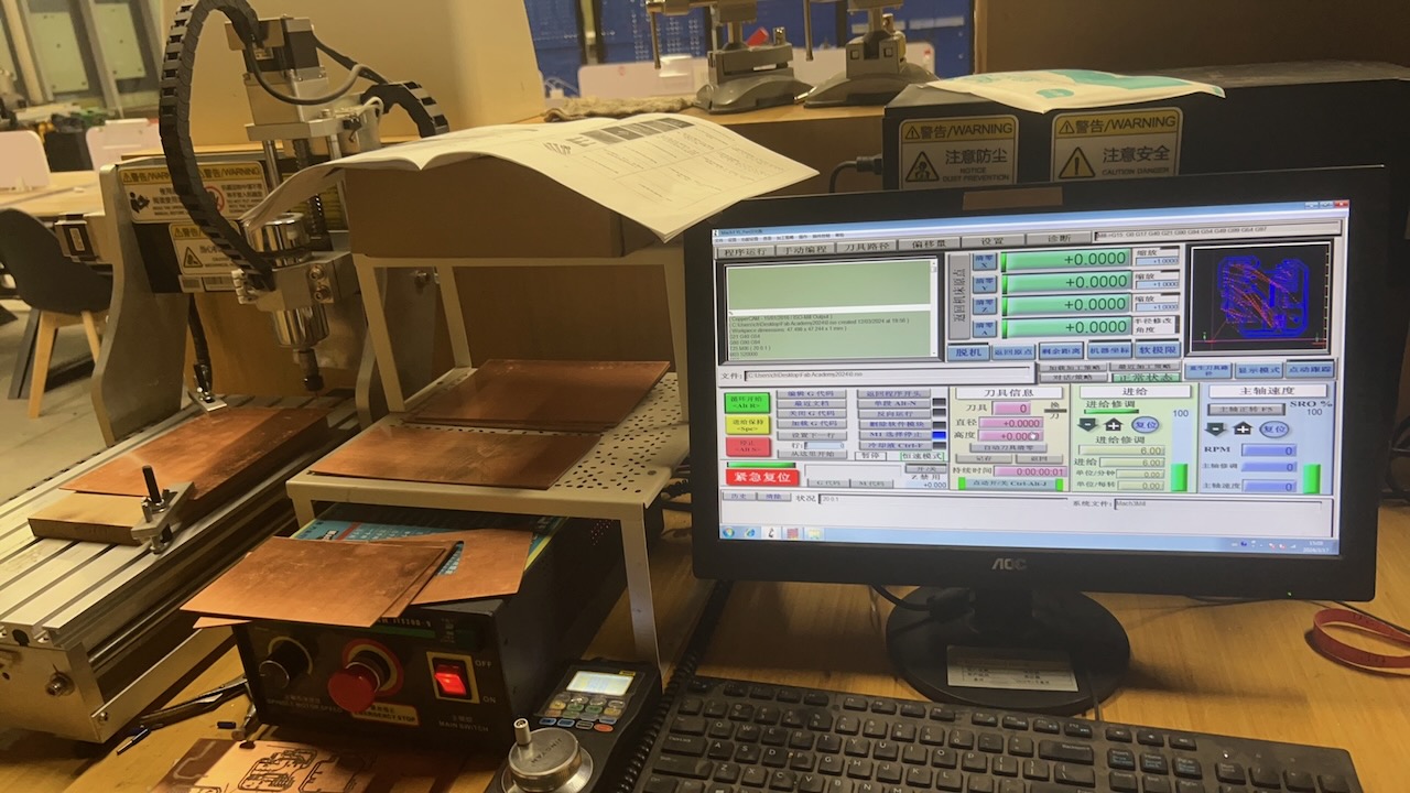
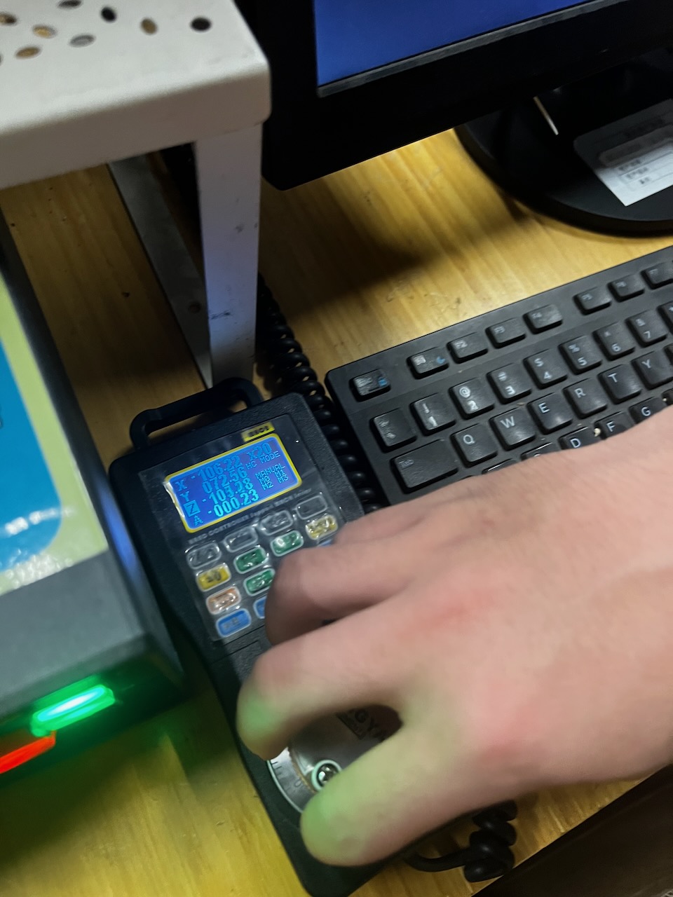
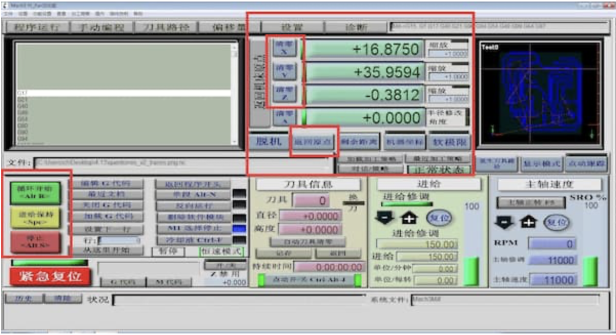
Software:Mach3 • Software to control the CNC machine, used for initializing the equipment, setting tool positions, and loading and executing G-code.
• Allows manual control of the machine’s movement and adjustment of spindle and feed rates.
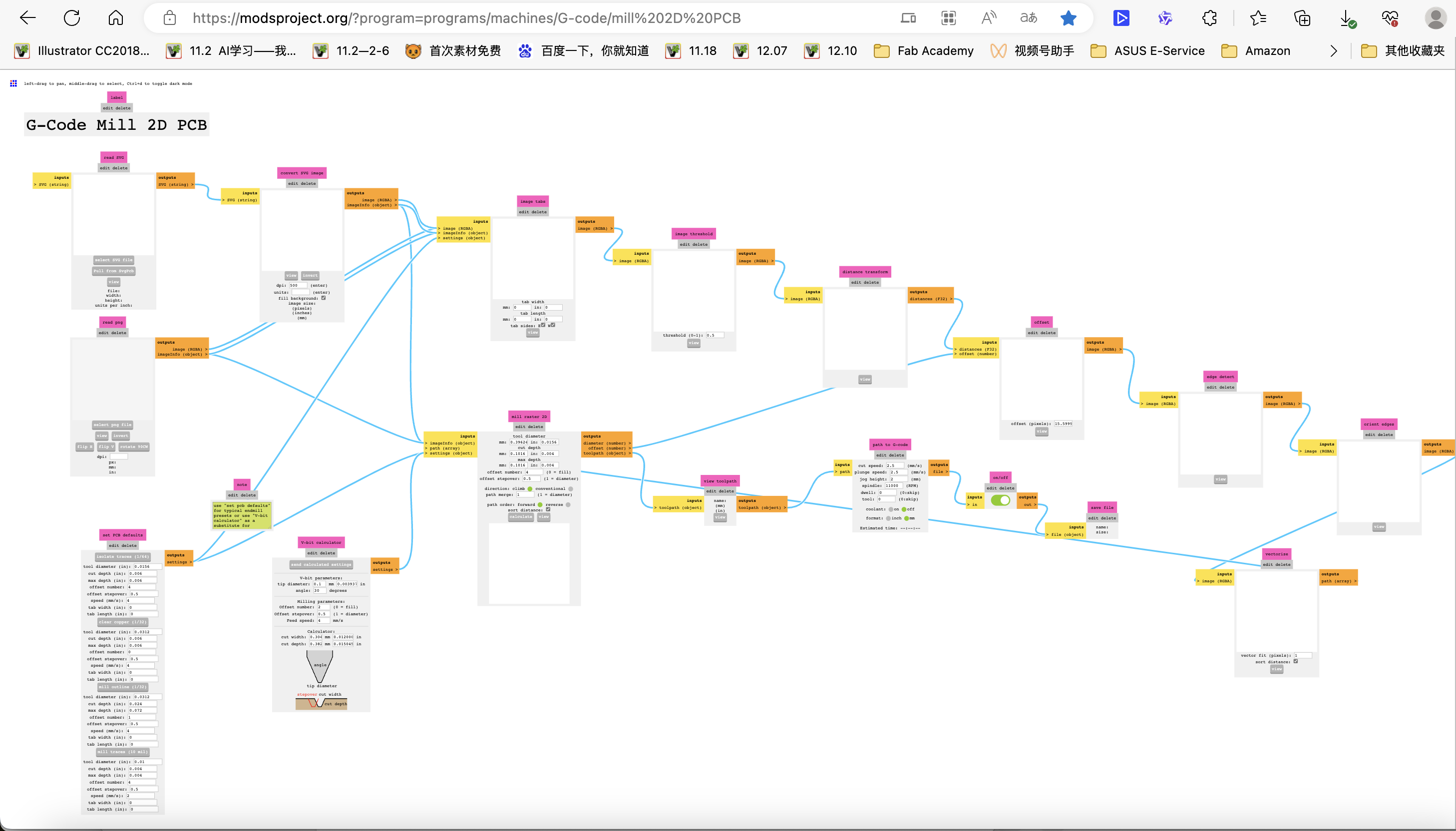
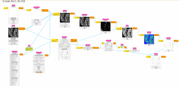
Software:G-Code Mill 2D PCB • An online tool for converting PNG images to G-code.
• Supports setting specific parameters like dots per inch (DPI) and tip diameter to accommodate different milling needs.
Software:Gerber2PNG • An online tool for converting Gerber files to PNG.
• Allows users to upload a Gerber file and convert it to a PNG image.
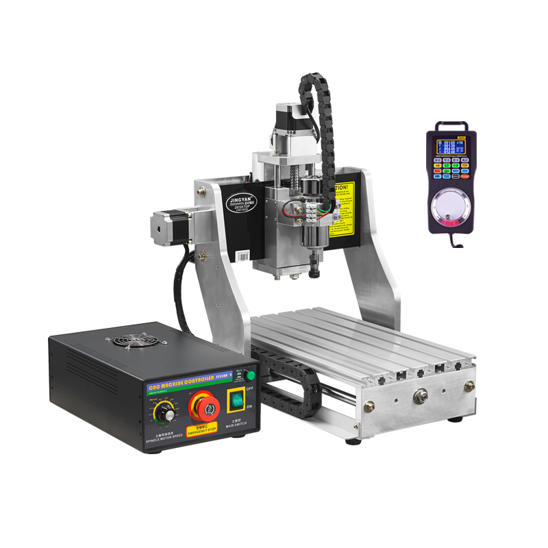
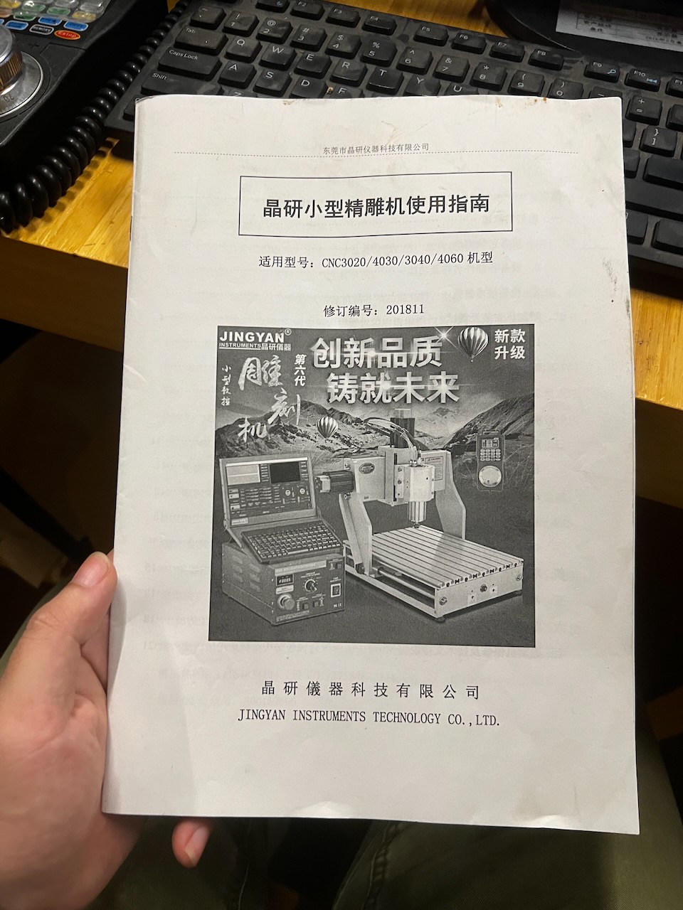
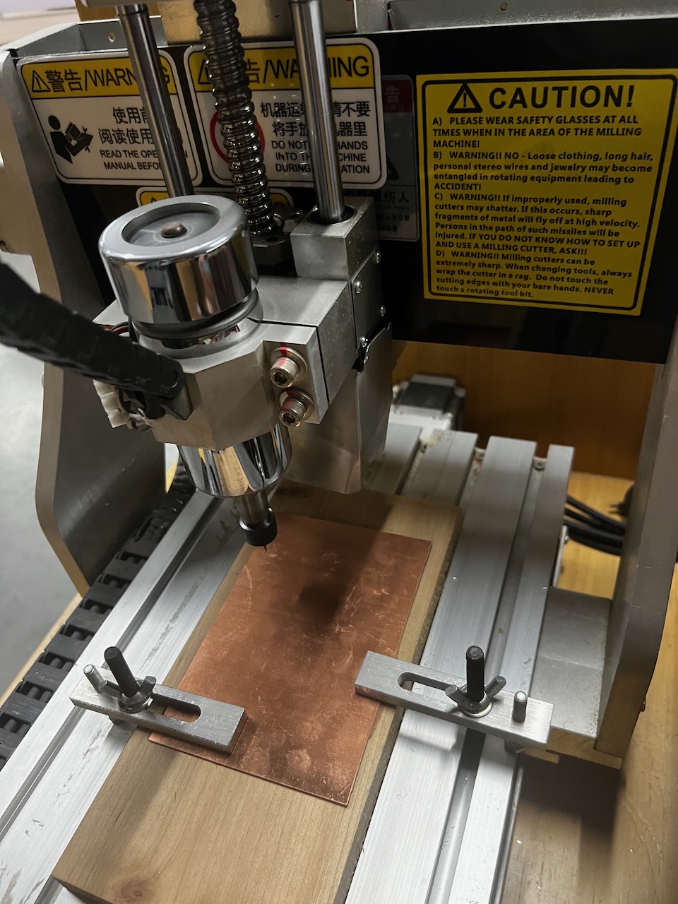
Machine:JING YAN CNC JING YAN CNC is a small CNC machine that can be used for PCB manufacturing.
The model in Chaihuo is JING YAN CNC-3020, which is a small Engraving Machine with 300w power and 300mm x 200mm working area.
Applicable Material: Copper, Aluminum and other soft metal,Plastic, Wood,Acrylic, PVC,PCB,etc....
Tools:
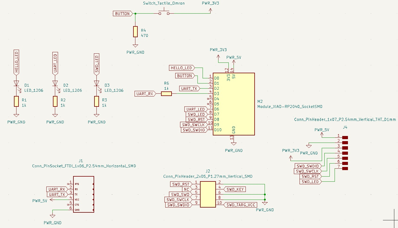
3.Learn the Schematic of Quentorres
and added them to the KiCad.
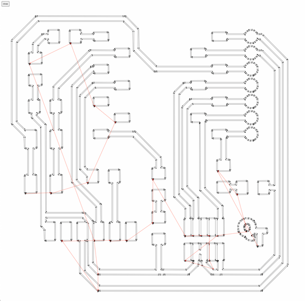
4.Learn the PCB files of Quentorres
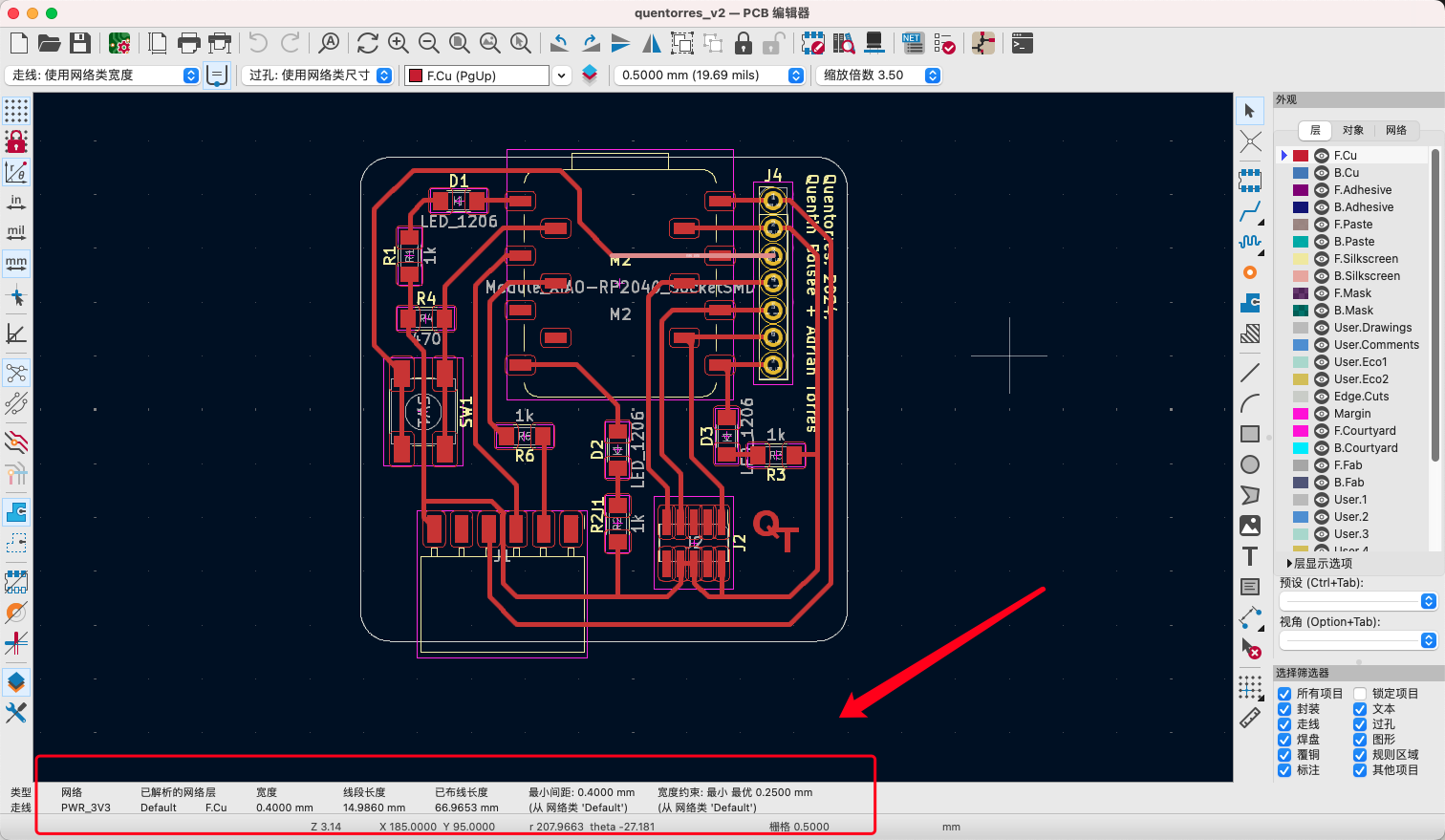
Grid: 2.54mm
Tickness:3.6mm
Nets: 24
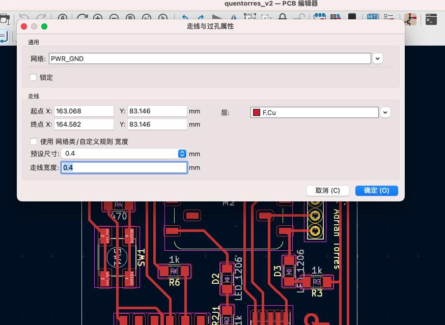
Width: 0.4mm
Pads: 57
5.From Gerber to G-Code
Converting from Gerber files to G-code files involves two steps:
1. Convert the Gerber files into recognizable PCB photoprint images.
2. Generate G-code files from the photoprint images.
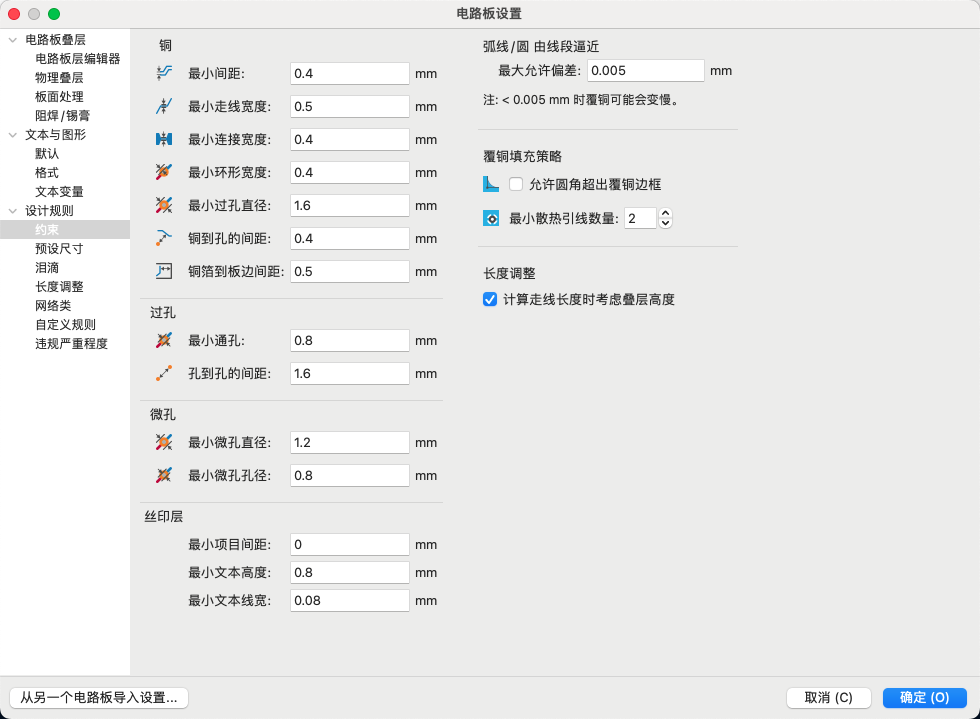
Please remember to adjust the PCB design rules, as we are using CNC machining for the PCB.
Pay attention to the minimum precision possible with CNC machining.
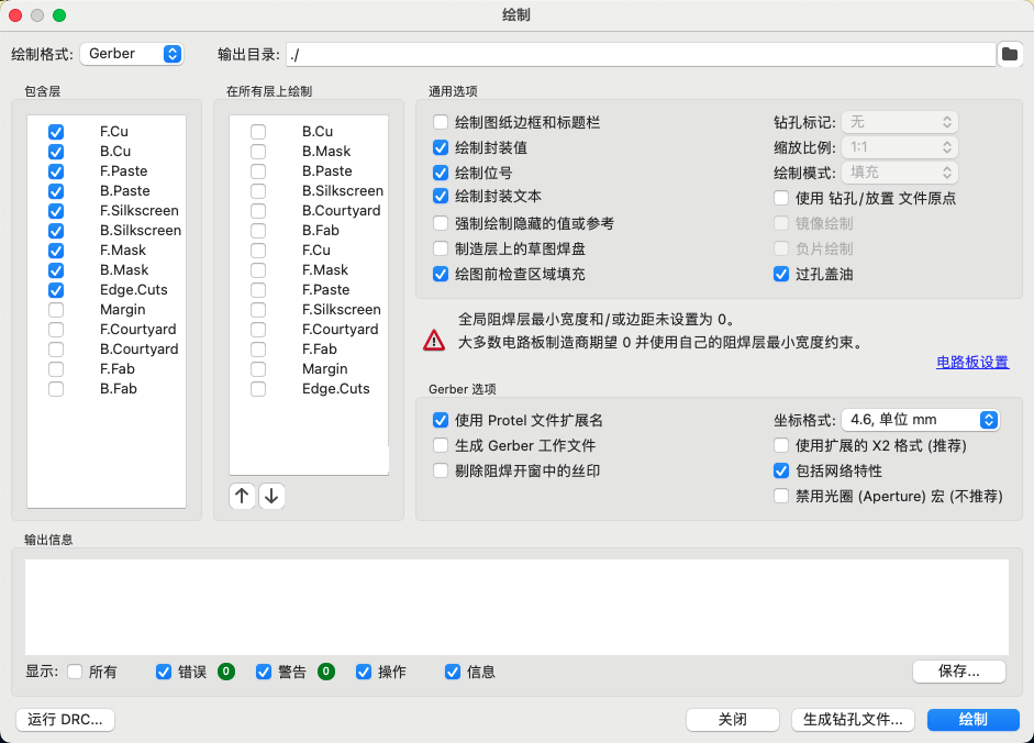
OK!We can get the manufacturing files.
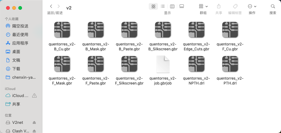
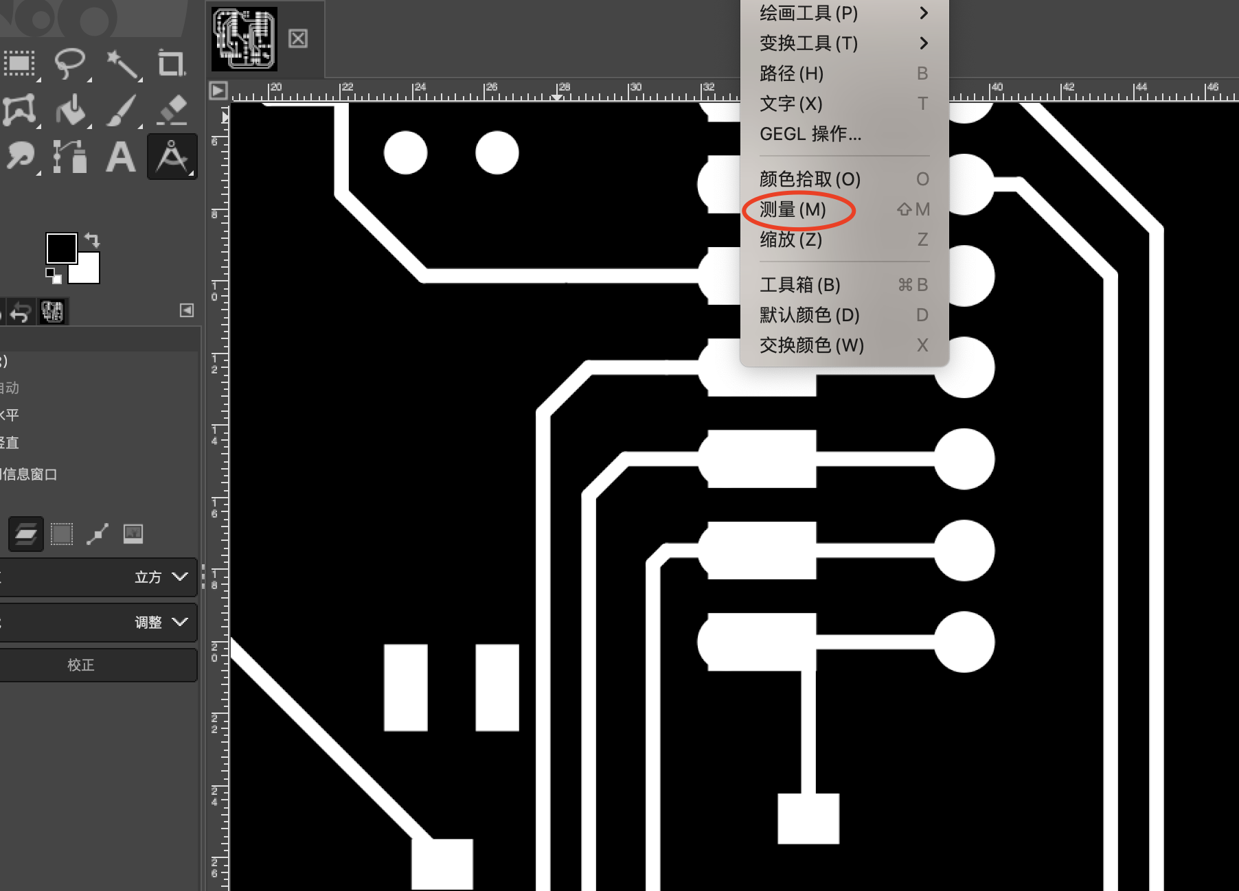
Then upload the Gerber files to the online tool Gerber2PNG to generate the PCB photoprint images.
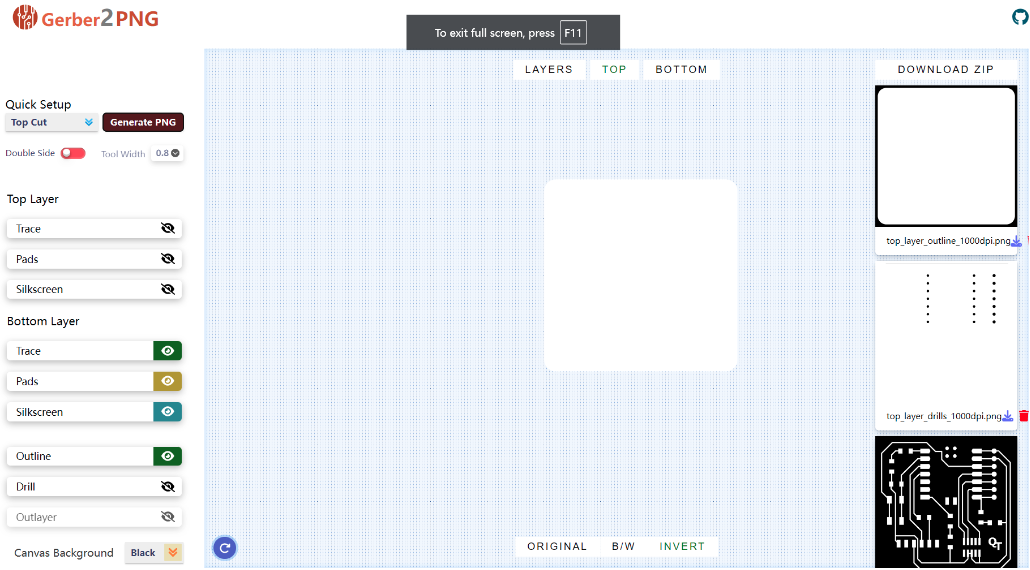
We need to get 3 images: traces, interior, and Drill.
QT PCB Photoprint images:
Traces:
.png)
Interior:

Drills:

 Special note:
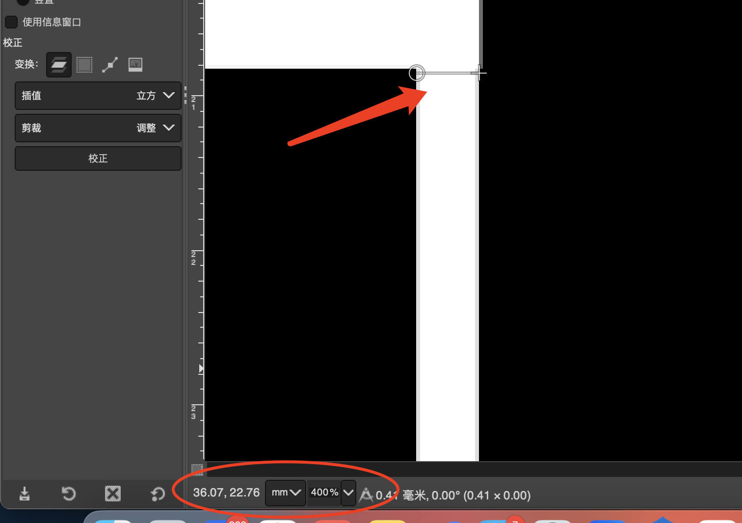
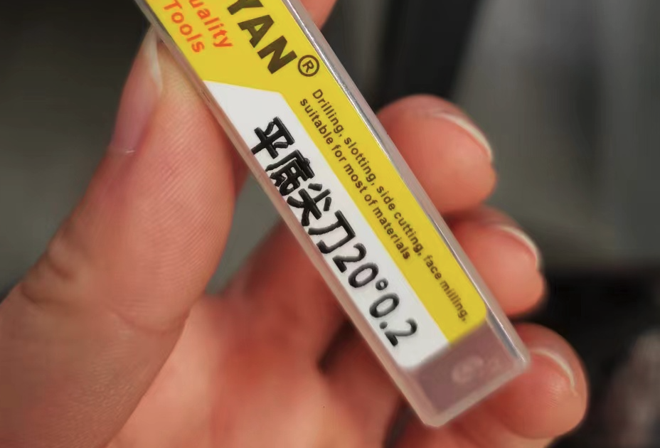
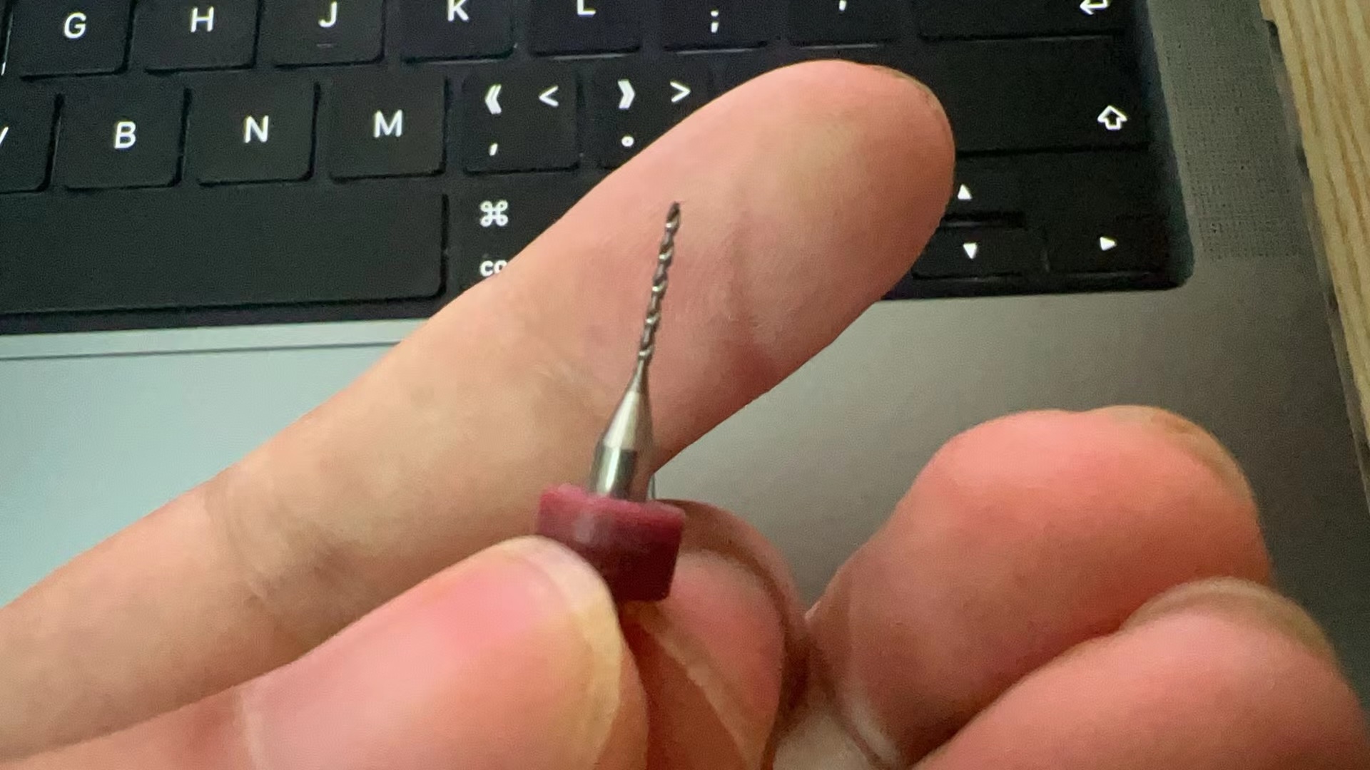
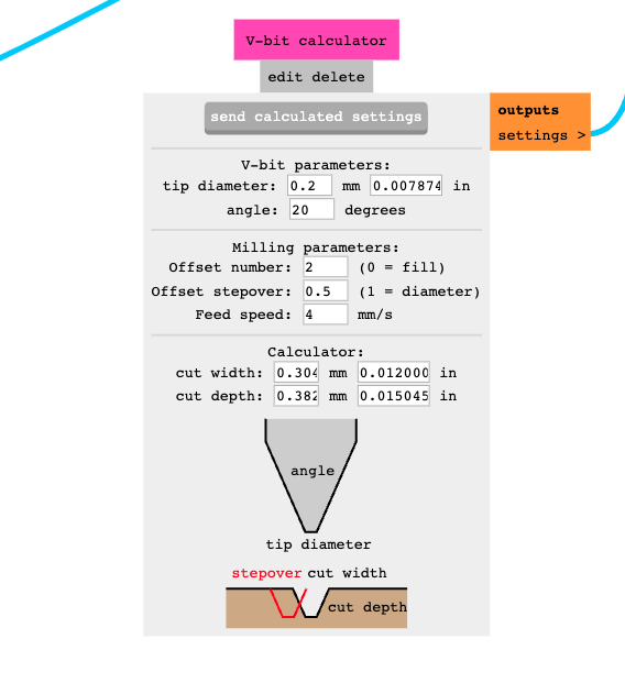
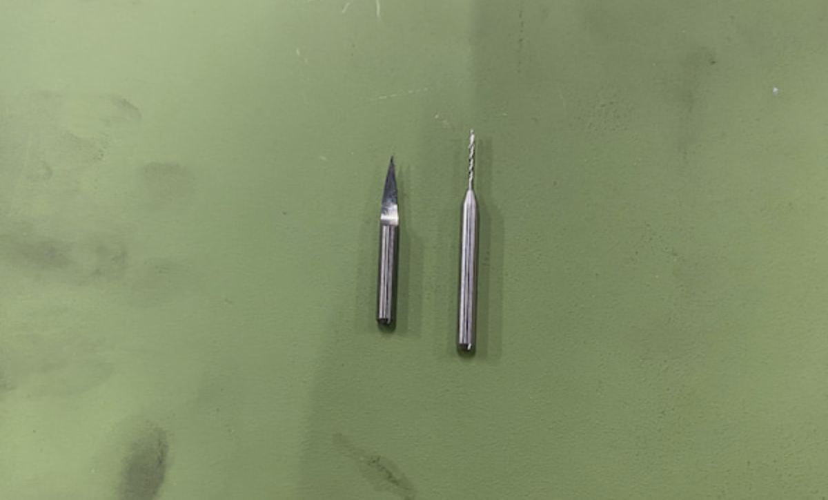
• Before setting up the machining files, please pay attention to the parameters of the engraving and drilling tools being used.
engraving tool: tip diameter--0.2mm Angle--20°
drilling tool: 0.8mm
Ultimately, we can obtain a preview of the G-code file.
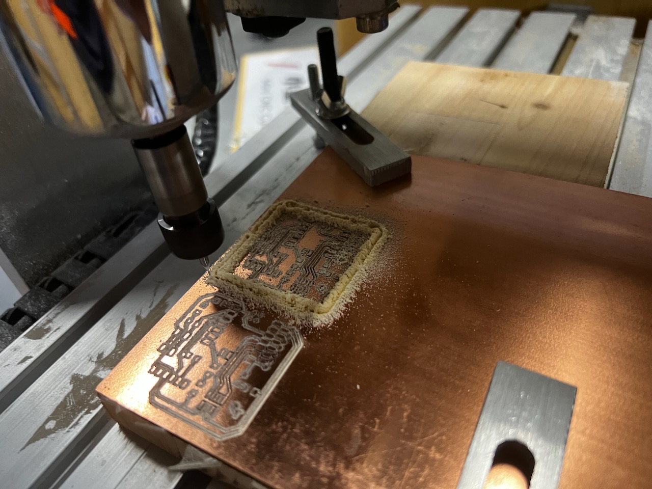
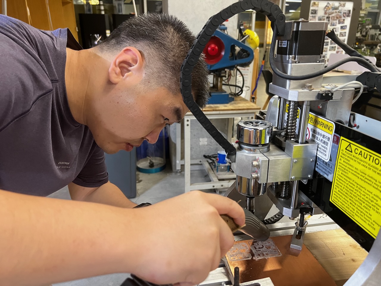
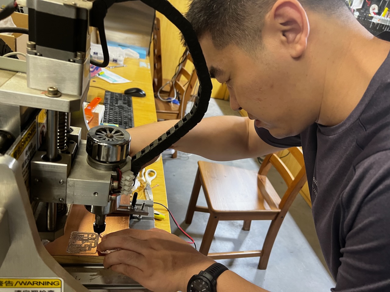
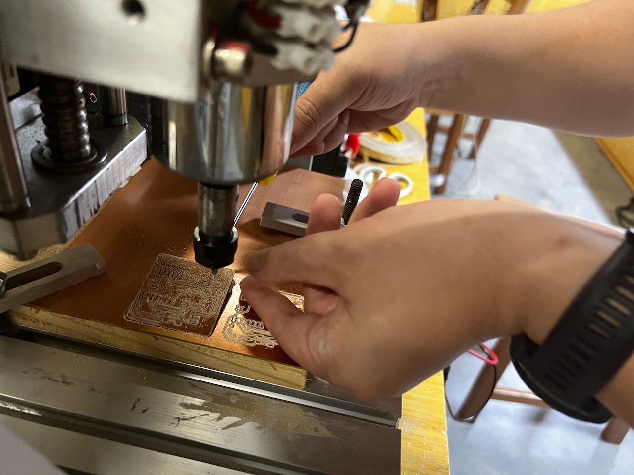
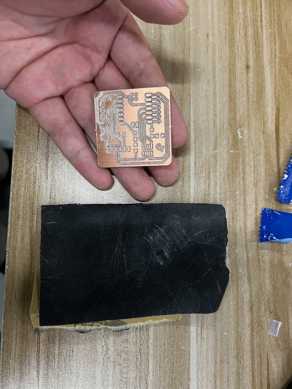
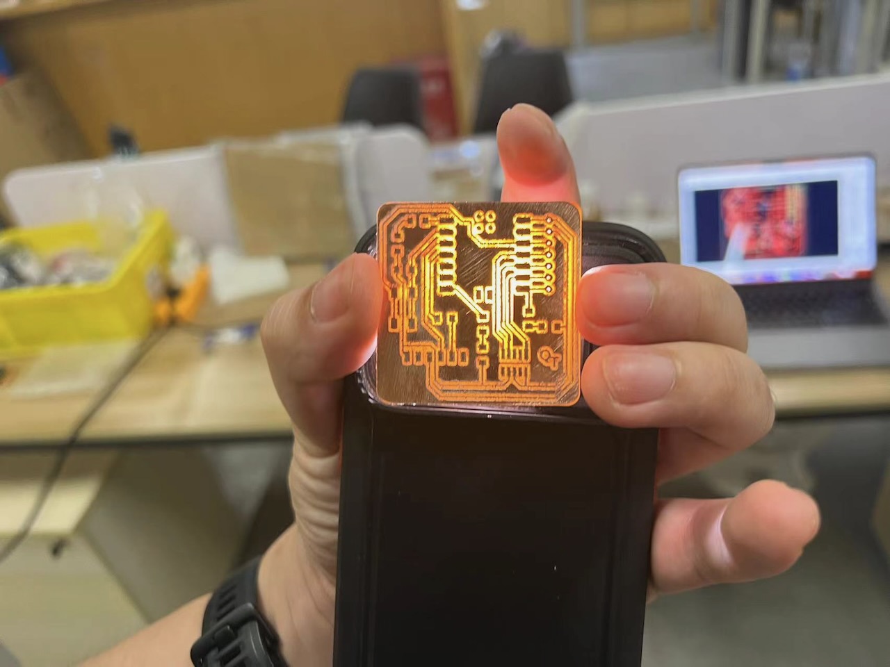
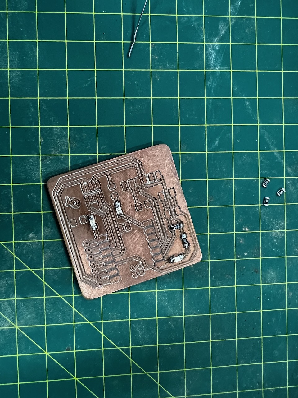
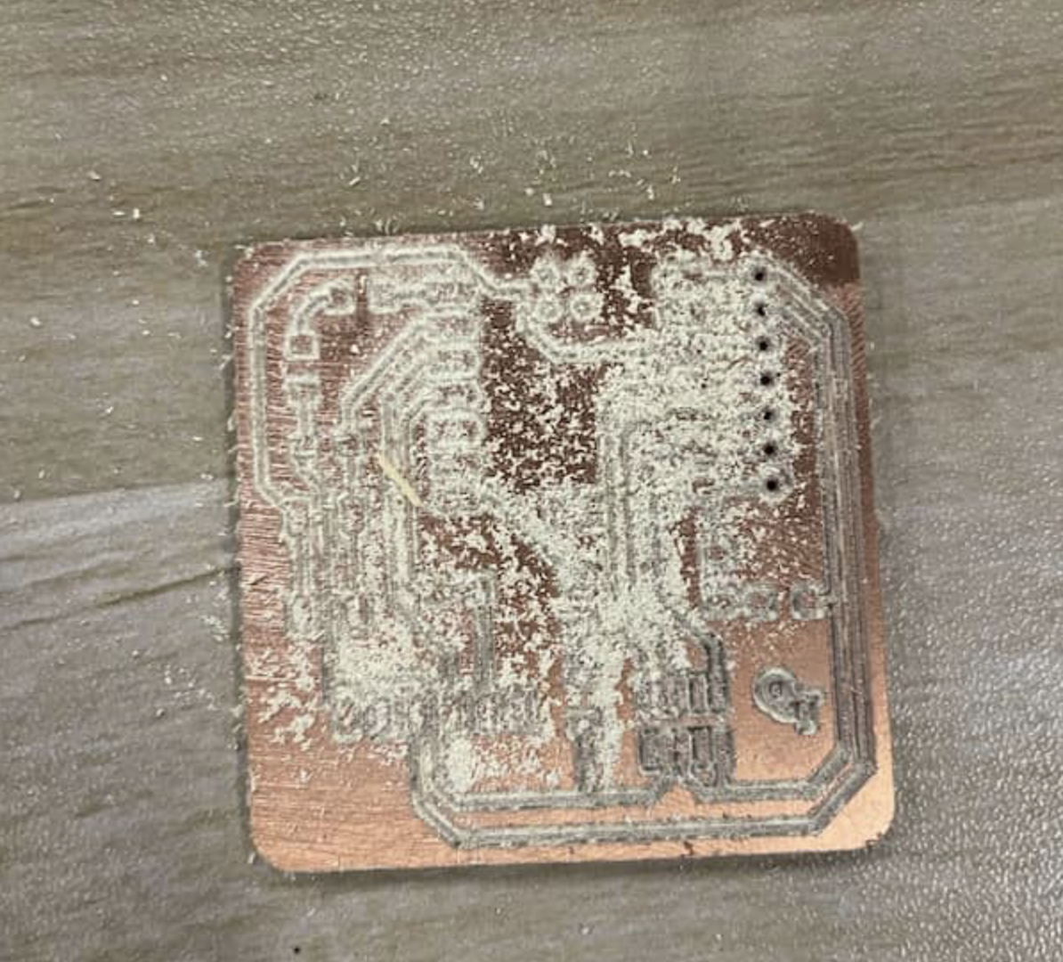
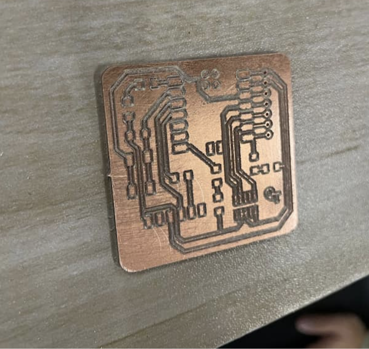
6.Machining the PCB
• Material Fixing: Use double-sided tape or a vise to secure the PCB material to be processed.
• Tool Loading: Choose appropriate V-bits or drills, mount them on the spindle, and lock them in place using the spindle wrench.
• Equipment Initialization: Use Mach3 software to power on the machine, clear alarms, and set the tool’s starting position.
• G-code Loading: Load G-code into Mach3, make final settings before machining, such as adjusting spindle speed and feed rate.
• Start Machining: Start the machine to begin processing, adjust feed rates as necessary and check the quality of machining.
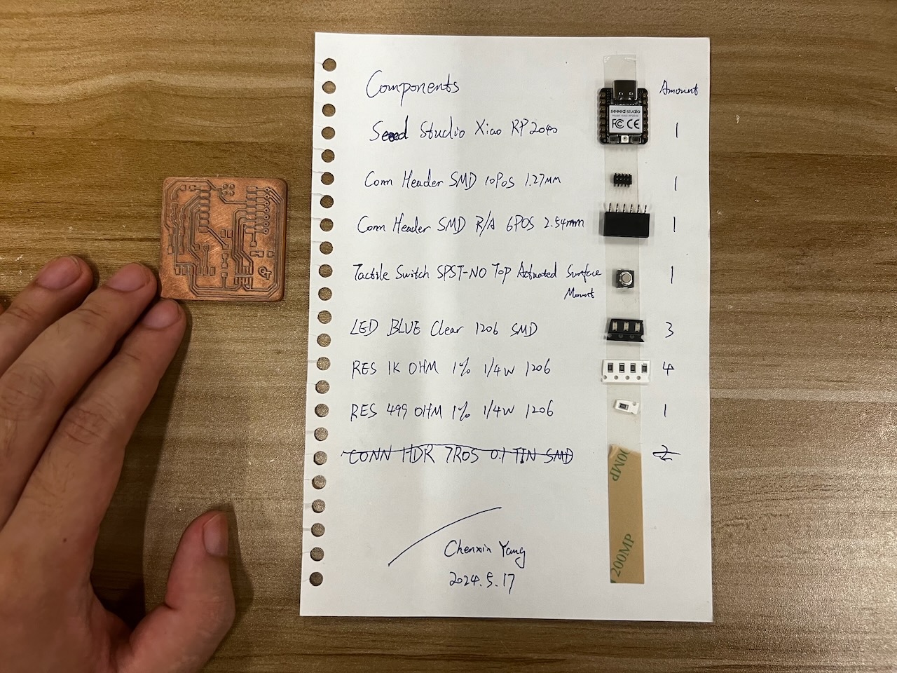
7.Make the BOM for QT PCB
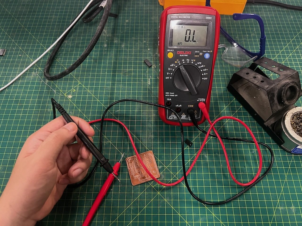
After completing the PCB machining, I used a multimeter to test the connectivity of the PCB circuits to ensure there were no short circuits.
The specific method involved using the circuit connectivity test function of the multimeter, testing all the wires one by one with the positive and negative probes.
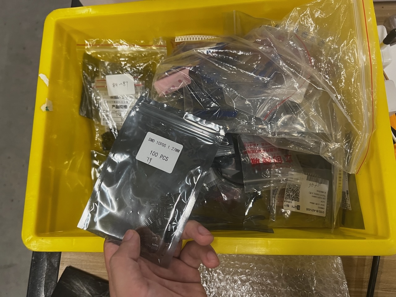
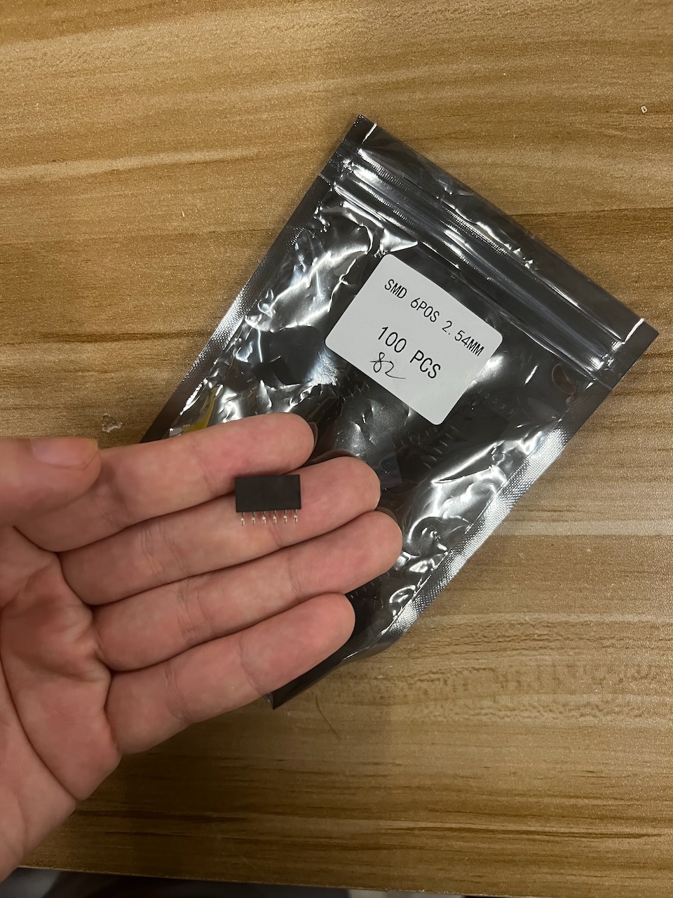
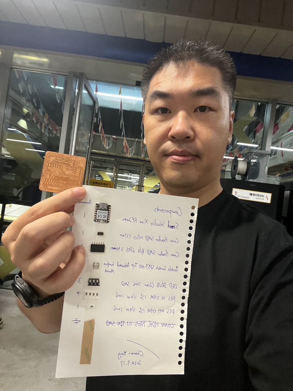
Here is the BOM (Bill of Materials) for QTv2.
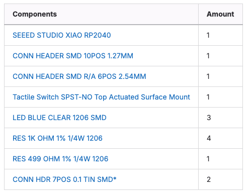
I found each required component from the component storage area one by one, organized them together, and made a list.
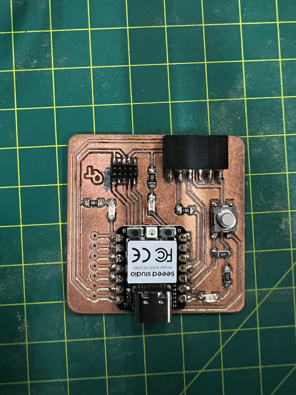
8.Solder components onto the PCB
• Component Placement: Position electronic components on the PCB as per the design.
• Soldering: Solder the components using soldering tools, ensuring good connections for all components.
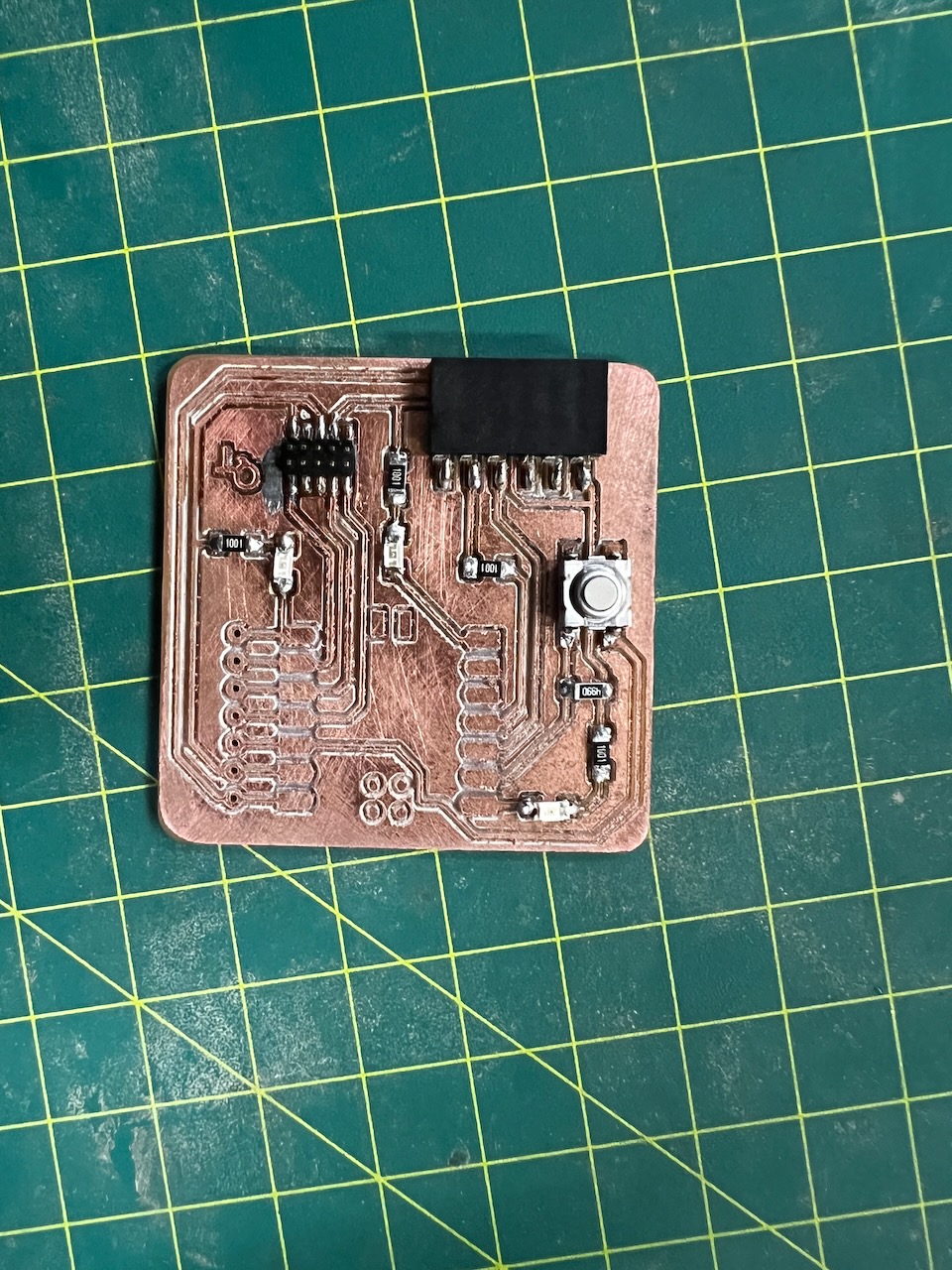
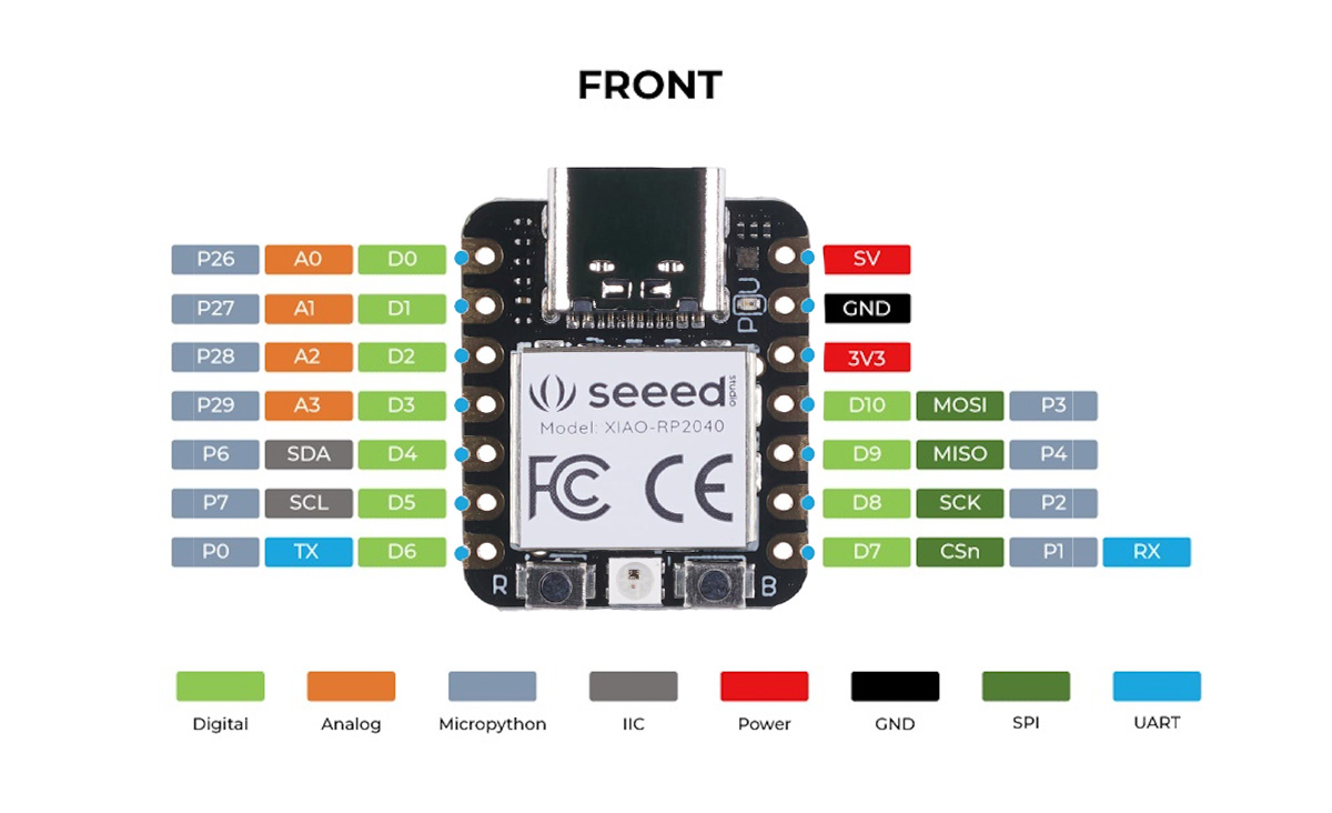
After completing the soldering of the main components, I began soldering the Xiao RP2040.
Below is the pinout manual for the Xiao RP2040.
Also, be sure to place an insulating sticker at the power pin location to prevent short circuits.
QTv2 soldering completed.
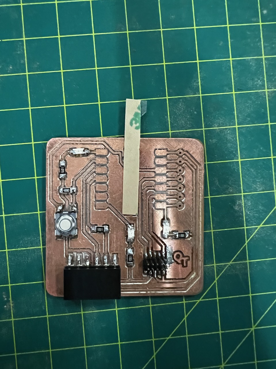
9.Testing:
• Multimeter Testing: Use a multimeter to check the PCB for any shorts or continuity issues, ensuring all circuits are correctly connected and functional.• Functional Testing: Power up the PCB and test its functionality as per the designed circuit behavior.
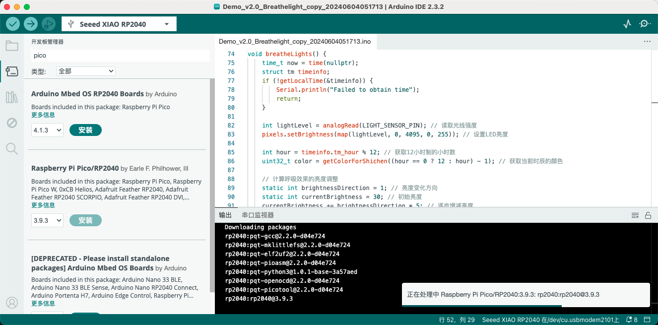
10.Write and test the program.
After completing the entire PCBA, I chose to use a blink program code to test whether this PCBA is functional.
Here is my code:
                          //Blink
                          void setup() {
                            // initialize digital pin LED_BUILTIN as an output.
                            pinMode(D1, INPUT);
                            pinMode(D0, OUTPUT);
                            pinMode(D6, OUTPUT);
                            pinMode(D7, OUTPUT);
                          }

                          // the loop function runs over and over again forever
                          void loop() {
                            int buttonState = digitalRead(D1);

                            if (buttonState == HIGH) {
                              // 如果按钮被按下,点亮所有LED
                              digitalWrite(D0, HIGH);
                              digitalWrite(D6, HIGH);
                              digitalWrite(D7, HIGH);
                            } else {
                              // 否则,熄灭所有LED
                              digitalWrite(D0, LOW);
                              digitalWrite(D6, LOW);
                              digitalWrite(D7, LOW);
                            }            // wait for a second
                          }
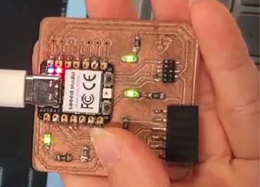
Connect tthe QT board to my laptop.
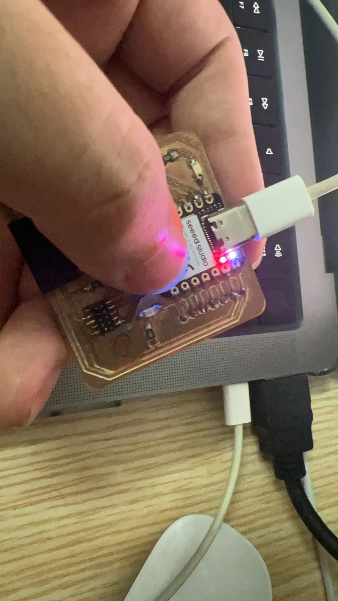
Find the platfrom RP2040 and install the Xiao RP2040 driver.
OK!light up the LEDs.
Team Assignment
1. Design and Preparation:
• Software Usage: Utilize KiCad, an Electronic Design Automation (EDA) tool, to design the PCB layout and generate necessary files like Gerber and drill files.

2. PCB Milling Preparation:
• Material Fixing: Secure the PCB material using double-sided tape or a vise on the Jingyan CNC Engraving Machine.
• Tool Setup: Install appropriate V-bits or drills, depending on the detail and depth required for the milling, using the spindle wrench to secure the tools.
3. Milling Process:
• Machine Setup: Initialize the machine using Mach3 software, setting the tool’s start position and loading the G-code.
• Machining: Start the CNC machine, carefully adjust spindle and feed rates as needed, and monitor the milling process to ensure precision and quality.
4. Post-Milling Operations:
• Inspection and Cleaning: After milling, inspect the PCB for any errors or misalignments and clean the board of any debris or residues.
Assignment files
Let's Jump to the Top !!!